
Technical information
TECHNOLOGY
Our company has specialized in the research, development, and manufacturing of functional photochemical materials for over 60 years.
Based on the photosensitive materials technology cultivated in the printing field, we have expanded our applications to the electronic and optical device fields, and now we supply materials essential for image sensors and semiconductor processes. Here, we introduce our representative technological fields and their characteristics.
Microlens materials
Improved light capture performance of the image sensor
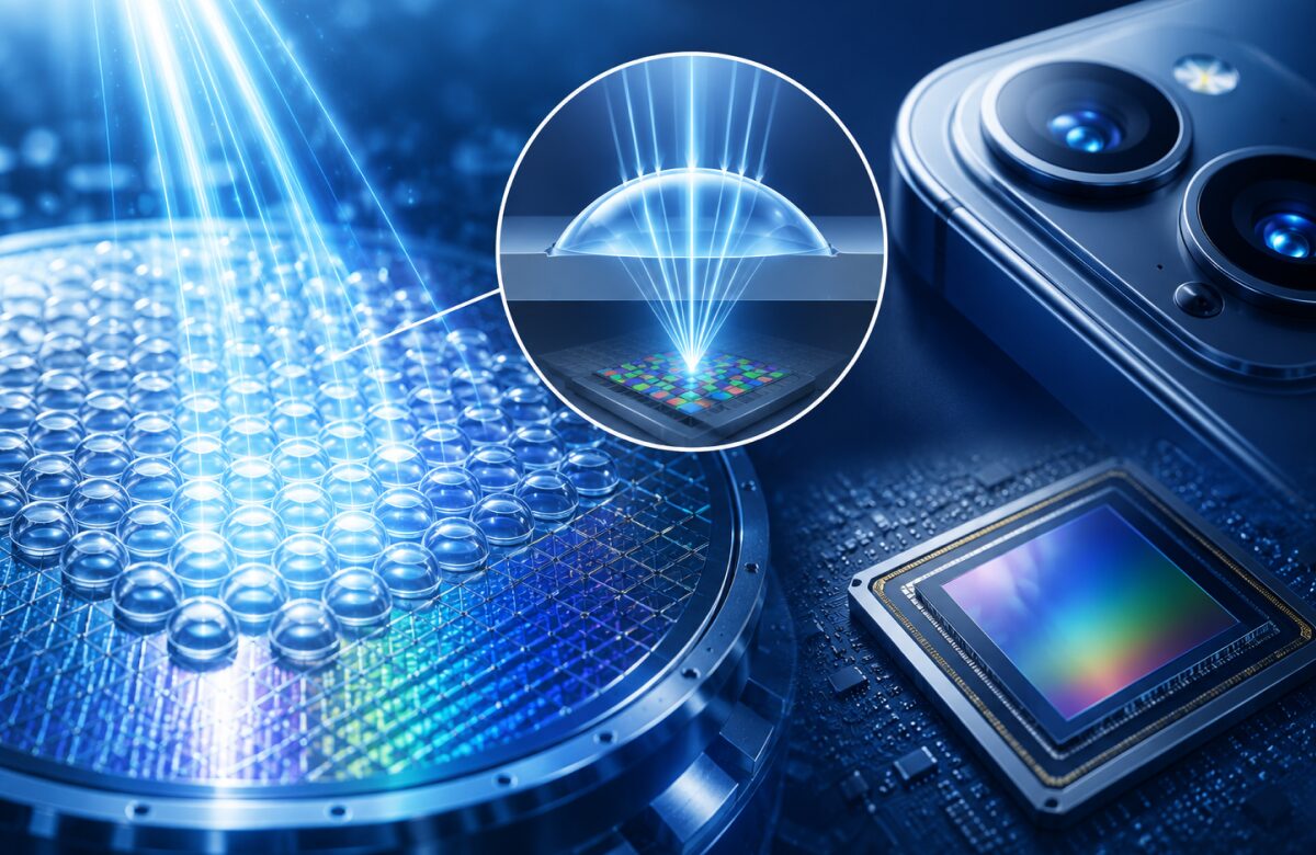
We have been developing and manufacturing microlens materials used in image sensors (CIS) for many years, contributing to improved imaging performance in smartphones and cameras. We offer a variety of materials to suit multiple process conditions.
Lift-off materials
Lift-off technology supporting microstructure formation
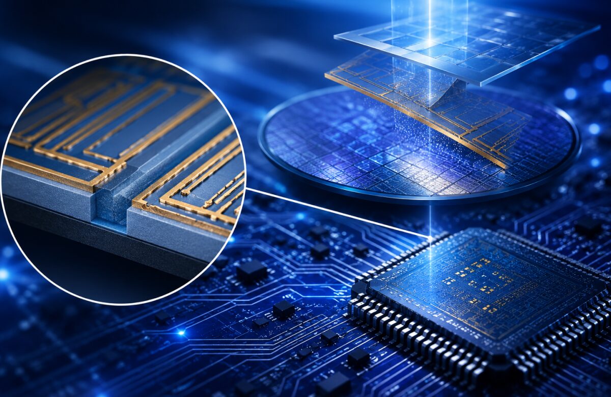
For over 30 years, we have provided high-resolution, high-manufacturing-margin lift-off materials.It supports the manufacturing of electronic components that require the formation of microstructures. Its key features include single-layer structure and the elimination of the need for inversion processes.
Photoresist materials (multiple varieties, continuous supply)
Wide variety and continuous supply
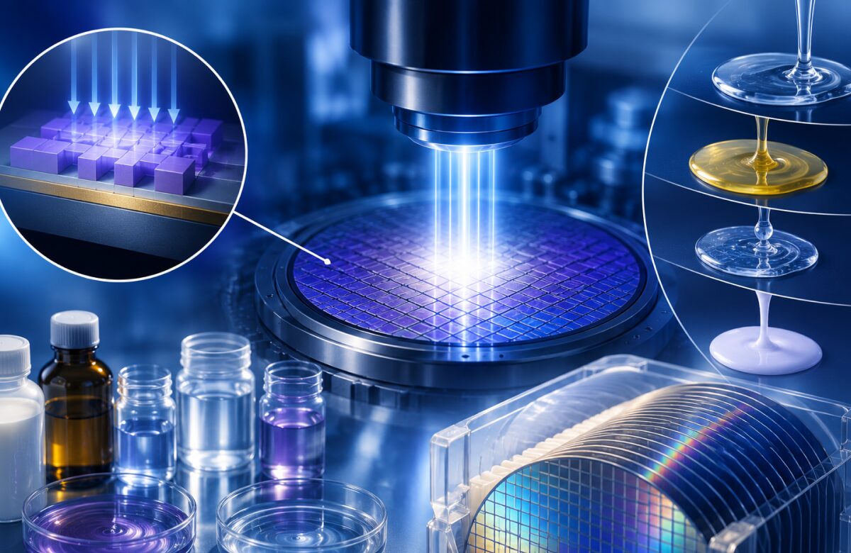
Since its founding, the company has continuously developed and manufactured a wide variety of photoresist materials. It has a system in place to supply a diverse range of materials with stable quality, including water-soluble photoresists and cyclic rubber-type resists with over 40 years of proven performance.
Photosensitive materials for printing
Fundamental technologies for image formation and exposure control
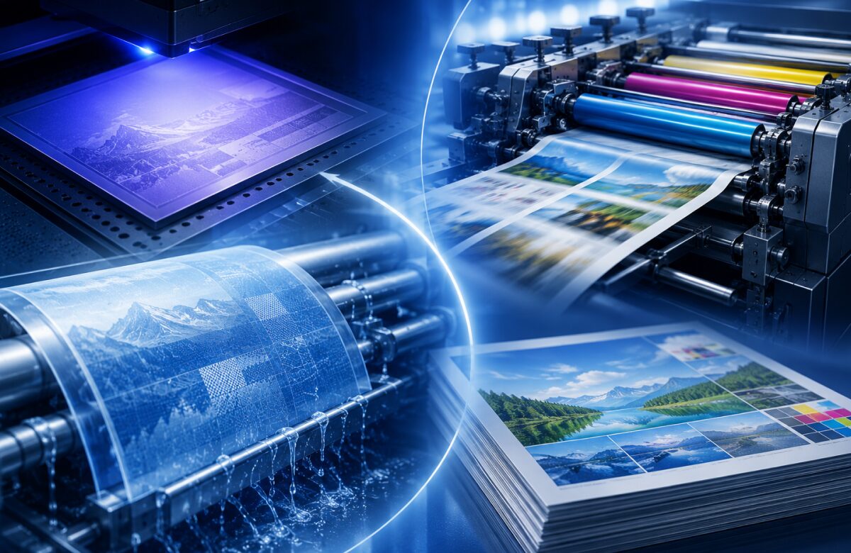
Through the development and manufacture of photosensitive materials used in the printing industry, we have accumulated many years of expertise in image formation and exposure/development processes. These technologies form the foundation for our materials development in the electronics and optics fields.